

Graphene Moves Closer to Replacing Chips With ‘Big Mac’ Structure
A team at Manchester University have developed a sandwich-like architecture of the material graphene that could see the material move closer to replacing silicon.
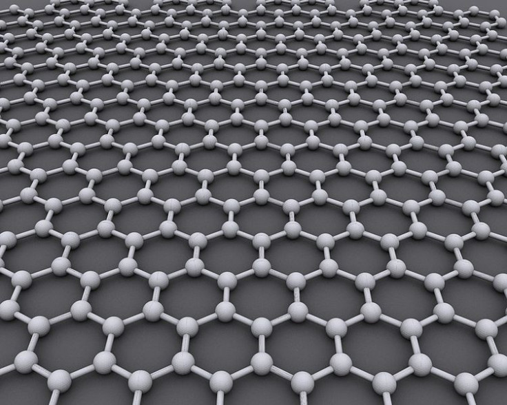
The "Big Mac" circuit architecture placed graphene - described as the world's thinnest, toughest and most conductive material - between sheets of another two-dimensional material boron nitrate to produce a four-layered structure which could replace silicon chips in computers.
Writing in the journal Nature Physics, the University of Manchester team have for the first time demonstrated how graphene inside electronic circuits could look in the future.
"Creating the multilayer structure has allowed us to isolate graphene from negative influence of the environment and control graphene's electronic properties in a way it was impossible before," said Leonid Ponomarenko, who led the study.
"It's technically important that our demonstration shows that graphene encapsulated within boron nitride offers the best and most advanced platform for future graphene electronics," said professor Andre Geim, who last year won a Nobel Prize for physics for his work on graphene.
"It solves several nasty issues about graphene's stability and quality that were hanging for long time as dark clouds over the future road for graphene electronics."
"We did this on a small scale but experience shows that everything with graphene can be scaled up," Geim said. "It could be only a matter of several months before we have encapsulated graphene transistors with characteristics better than previously demonstrated."
Its remarkable properties could lead to bendy, touch screen phones and computers, lighter aircraft, wallpaper-thin HD TV sets and superfast internet connections.
The £50m Graphene Global Research and Technology Hub will be set up by the Government to commercialise graphene.
© Copyright IBTimes 2024. All rights reserved.


