World's smallest transistor enables scientists to push the laws of physics further
Scientists have challenged the laws of physics by creating a 1 nanometre transistor gate for semiconductors.

Scientists from University of California Berkeley (UC Berkeley) have pushed the laws of physics to the hilt by shrinking the size of electronics even further with the development of the world's smallest transistor.
Currently transistors in a high-end semiconductor on the market measure between 20-22 nanometres (nm) in size. Electronics keep getting smaller and it is predicted that we will have 10nm transistor gates in consumer products in 2017, with 5nm transistor gates possible in 2021. To give you perspective, a single strand of human hair is 50,000 nanometres thick.
However, the laws of physics predict that if you shrink transistors any smaller than 5nm, electrons flowing along a conductor can 'hop across' to the next conductor, making it impossible to control the electrical current – a phenomenon known as quantum tunnelling.
It is believed 5nm transistor gates will posit a direct challenge and in fact bring about the end of the already established Moore's Law – an observation that the number of transistors in a dense integrated circuit double approximately every two years.
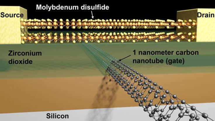
UC Berkeley scientists decided to work with a material that is not silicon – which is the traditional substrate for electronics – namely carbon nanotubes and molybdenum disulphide (MoS2). MoS2 is an engine lubricant found in automobile repair shops – part of a family of materials which are resistant to conductivity, it shows great promise for use in lasers, solar cells and LEDs.
"The semiconductor industry has long assumed that any gate below 5 nanometres wouldn't work, so anything below that was not even considered," said study lead author Sujay Desai, a graduate student at Berkeley Lab's Materials Science Division in UC Berkeley.
"This research shows that sub-5-nanometre gates should not be discounted. Industry has been squeezing every last bit of capability out of silicon. By changing the material from silicon to MoS2, we can make a transistor with a gate that is just 1 nanometre in length, and operate it like a switch."
Both silicon and MoS2 have crystalline lattice structures, but quantum tunnelling occurs more in silicon as the electrons encounter less resistance than in MoS2. Still, because it is difficult to get conventional lithography techniques to work at 1nm, the scientists had to use carbon nanotubes in order to control the flow of the electrons.
"We made the smallest transistor reported to date," said Ali Javey, lead principal investigator of the Electronic Materials programme in Berkeley Lab's Materials Science Division. "The gate length is considered a defining dimension of the transistor. We demonstrated a 1-nanometer-gate transistor, showing that with the choice of proper materials, there is a lot more room to shrink our electronics."
Although this is exciting news, scientists warn that it is only a proof of concept. While it is possible to make transistor gates for semiconductors that are smaller than 5nm, before this concept can be realised, scientists will need to pack the transistors onto a chip and get it to work.
Their research, entitled 'MoS2 transistors with 1-nanometer gate lengths' is published in the journal Science.
© Copyright IBTimes 2025. All rights reserved.
- MOST READ